

")


09-26
GaN Single Crystal Substrate For High Power Devices
Products Center
4" self-supporting GaN wafers (non-doped)
Specification: GaN-FS-C-U-C100
Size:Ф 100 ± 0.1 mm
Thickness:650 ± 50 μm
Resistivity (300k): < 0.5 Ω*cm


4-inch self-supporting GaN wafers (iron doped)
Specifications:GaN-FS-C-SI-C100
Size:Ф 100 ±1 mm
Thickness:420 ±50μm
Resistivity(300k): >1×10⁹Ω*cm
2" self-supporting GaN wafers (non-doped)
Specifications: GaN-FS-C-U-C50
Size:Ф 50.8 ± 1 mm
Thickness:350 ± 25 μm
Resistivity (300k): < 0.5 Ω*cm
4" self-supporting GaN wafers (non-doped)
Specification: GaN-FS-C-U-C100
Size:Ф 100 ± 0.1 mm
Thickness:650 ± 50 μm
Resistivity (300k): < 0.5 Ω*cm
4-inch self-supporting GaN wafers (iron doped)
Specifications:GaN-FS-C-SI-C100
Size:Ф 100 ±1 mm
Thickness:420 ±50μm
Resistivity(300k): >1×10⁹Ω*cm
2" self-supporting GaN wafers (non-doped)
Specifications: GaN-FS-C-U-C50
Size:Ф 50.8 ± 1 mm
Thickness:350 ± 25 μm
Resistivity (300k): < 0.5 Ω*cm

Company Introduction
Since the establishment of Suzhou Nanowin Science and Technology Co., Ltd, with the support of major achievement transformation projects in Jiangsu Province and talent projects at all levels in Suzhou City, after 10 years of research and development, we have completed the complete process development from the independent research and development of material growth equipment to the growth and preparation of GaN single crystal substrate, and the dislocation density of 2-inch GaN single crystal substrate has been reduced to 10⁴cm², reaching the world advanced level. In the past two years, we have completed the key technology development of 4-inch and 6-inch GaN single crystal substrates. At present, GaN single crystal substrate products have been provided to more than 500 customers, basically completed the occupation of the R & D market, is to enhance the production capacity to the enterprise application market development, the key breakthrough direction is blue-green semiconductor laser, high-power power electronic devices, high reliability and high-power microwave devices and other major areas.
Professional supplier of high quality GaN substrates
Ltd. is dedicated to the R&D and industrialization of GaN single crystal substrate, the key material of the third generation semiconductor. Now we are one of the few domestic and international units that can provide 2-inch GaN single crystal products in batch; the comprehensive performance index of GaN products is leading in the world, and in the next three years, we will focus on transforming our technological first-mover advantage into global market advantage.
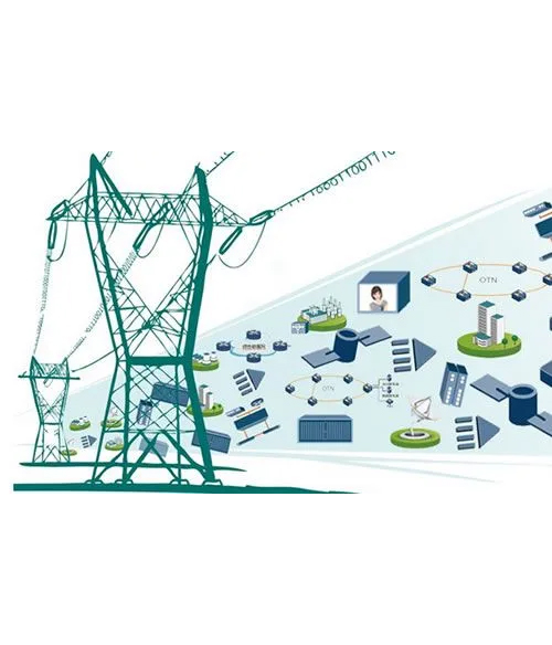
Ltd. was established in 2007, focusing on the growth of high quality GaN semiconductor single crystal materials. Gallium Nitride is the representative of the third generation semiconductor, it is the core basic material for energy-saving lighting, laser projection display, smart grid, new energy vehicles, 5G communication and other industries, and is expected to form a trillion dollar market in the future.
2007Year
Established
Established
500+
Clients Served
Clients Served
60+
Core Patents
Core Patents
50+
Invitation to Report
Invitation to Report
10billion+
Total Investment
Total Investment
Applications
Gallium Nitride is the representative of the third generation semiconductor, it is the core basic material for energy-saving lighting, laser projection display, smart grid, new energy vehicles, 5G communication and other industries, and it is expected to form a trillion dollar market scale by the future...
News Center
Contact Us
Add:Room 518, Building 20, Northwest District, Suzhou Nano City, No.99 Jinjihu Avenue, Suzhou Industrial Park
Customer service:
Miss Ren: 17712482910
Email: renjing@nanowin.com.cn
Sales Director:
Dai Dongyun: 15962257010
Email: daidongyun@nanowin.com.cn
Online Message
客户留言
Description:
 159-6225-7010
 Online Inquiry
Copyright © 2022 Suzhou Nanowin Science and Technology Co., Ltd 苏ICP备11034975号-1