

Gallium nitride single crystal in new display applications: microLED technology
- Categories:Application areas
- Time of issue:2022-09-26 10:49:58
- Views:0
Description:
Information
- GaN single crystal: smaller size, higher resolution, chip wavelength uniformity, smaller leakage current, higher efficiency under low current drive, homogeneous epitaxial MicroLED technology on the road to "Moore's Law".
 |
 |
WLD=472.5nm,std=0.9nm |
WLD=472.5nm,std=0.9nm |
|
Wavelength uniformity of homogeneous epitaxial chips on GaN single crystal substrates helps to solve the massive binning problem and the giant transfer problem. |
Chips with homogeneous epitaxy on GaN single crystal substrates exhibit better luminescence uniformity. |
 |
 |
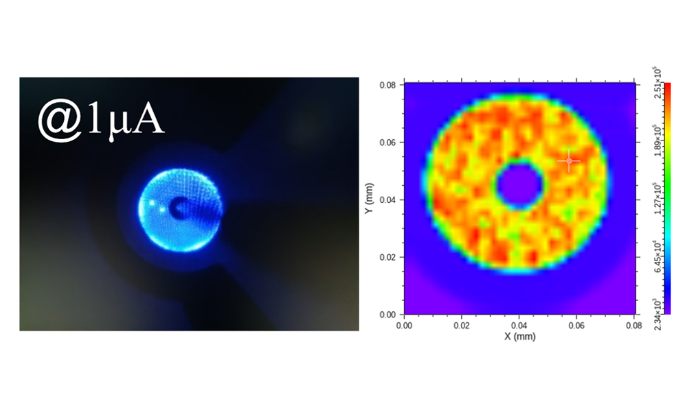
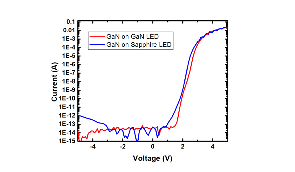
| Smaller leakage currents | Higher efficiency with low current drive |
GaN single crystal in new display applications: laser projection displays
- GaN single crystal: GaN single crystal substrate is the only substrate technology for the laser display technology route.
 |
 |
 |
|
VR眼镜 |
手机投影 |
汽车显示 |
 |
 |
 |
| Laser displays | Laser Cinema | Projection |
Contact Us
Add:Room 518, Building 20, Northwest District, Suzhou Nano City, No.99 Jinjihu Avenue, Suzhou Industrial Park
Customer service:
Miss Ren: 17712482910
Email: renjing@nanowin.com.cn
Sales Director:
Dai Dongyun: 15962257010
Email: daidongyun@nanowin.com.cn
Online Message
客户留言
Description:
 159-6225-7010

 Online Inquiry
Copyright © 2022 Suzhou Nanowin Science and Technology Co., Ltd 苏ICP备11034975号-1